
3. Specification – Interfaces and Wiring
Streszczenie: Specyfikacja, część 1 – interfejsy: dla każdego z 16 modułów ST-1xxx opis panelu, schemat podłączenia łączników i czujników 2- i 3-przewodowych (opisany tekstem) oraz tabela przypisania pinów.
EN: Specification, part 1: front panel, wiring diagram (described in text) and pin assignment for each of the 16 ST-1xxx modules.
Dotyczy: moduły wejść cyfrowych CREVIS serii ST-1xxx systemu FnIO (4, 8 i 16 wejść; 5, 12/24, 48 Vdc oraz 110/220 Vac)
Źródło: dokumentacja producenta (CREVIS ST-1xxx Digital Input Modules User Manual); tabele przepisane z obrazów na tekst, opisy rysunków – opracowanie Multiprojekt
Rozdział 3 „Specification” podzielono na 2 strony: Interfaces and Wiring · Technical Data.
3.1 The Interface
3.1.1 ST-1114
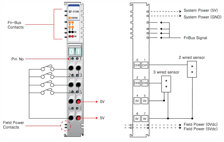
Diagram description (text version): ST-1114 (4 inputs, sink/positive logic, 5 Vdc): front view with FnBus contacts on the left side, STATUS LED and channel LEDs 0–3, and the 8-pin terminal block. Input switches are connected between the inputs (pins 0–3) and +5 V (pins 6/7); pins 4/5 are field ground 0 V. The wiring diagram shows a 2-wire sensor connected between CH1 and 5 V and a 3-wire sensor connected to CH2, 0 V and 5 V. System power (5 V, GND) and the FnBus signal come from the FnBus contacts; field power (0 Vdc / 5 Vdc) is taken from the field power contacts.
ST-1114 – pin description
| Pin No. | Description |
|---|---|
| 0 | Input Channel 0 |
| 1 | Input Channel 1 |
| 2 | Input Channel 2 |
| 3 | Input Channel 3 |
| 4 | Field Ground (0V) |
| 5 | Field Ground (0V) |
| 6 | Field Power (+5Vdc) |
| 7 | Field Power (+5Vdc) |
3.1.2 ST-111F
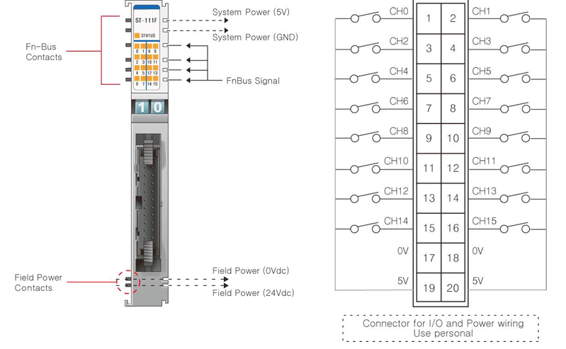
Diagram description (text version): ST-111F (16 inputs, sink/positive logic, 5 V): front view with FnBus contacts (system power 5 V/GND and FnBus signal), STATUS LED, 16 channel LEDs and a 20-pin connector for I/O and power wiring. Connector pinout: pins 1–16 – inputs CH0–CH15 (odd pins CH0, CH2 … CH14, even pins CH1, CH3 … CH15), pins 17/18 – 0 V, pins 19/20 – 5 V. Each input is wired through a switch to the common line, which is connected to 5 V (pins 19/20). The field power contacts at the bottom of the module are labelled Field Power (0 Vdc) and Field Power (24 Vdc) in the drawing.
ST-111F – pin description
| Pin No. | Description |
|---|---|
| 1 | Input Channel 0 |
| 2 | Input Channel 1 |
| 3 | Input Channel 2 |
| 4 | Input Channel 3 |
| 5 | Input Channel 4 |
| 6 | Input Channel 5 |
| 7 | Input Channel 6 |
| 8 | Input Channel 7 |
| 9 | Input Channel 8 |
| 10 | Input Channel 9 |
| 11 | Input Channel 10 |
| 12 | Input Channel 11 |
| 13 | Input Channel 12 |
| 14 | Input Channel 13 |
| 15 | Input Channel 14 |
| 16 | Input Channel 15 |
| 17 | Field Ground (0V) |
| 18 | Field Ground (0V) |
| 19 | Field Power (+5Vdc) |
| 20 | Field Power (+5Vdc) |
3.1.3 ST-1124
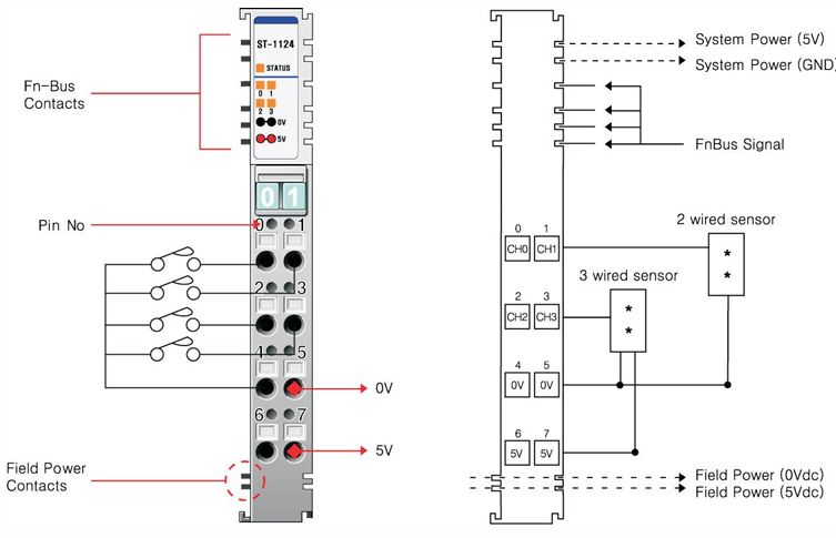
Diagram description (text version): ST-1124 (4 inputs, source/negative logic, 5 V): front view with FnBus contacts on the left side, STATUS LED, channel LEDs 0–3 and the 8-pin terminal block. Input switches are connected between the inputs (pins 0–3) and 0 V (pins 4/5); pins 6/7 are field power +5 V. The wiring diagram shows a 2-wire sensor between CH1 and 0 V, and a 3-wire sensor connected to CH2, 0 V and 5 V. System power (5 V, GND) and the FnBus signal come from the FnBus contacts; field power is taken from the field power contacts.
ST-1124 – pin description
| Pin No. | Description |
|---|---|
| 0 | Input Channel 0 |
| 1 | Input Channel 1 |
| 2 | Input Channel 2 |
| 3 | Input Channel 3 |
| 4 | Field Ground (0V) |
| 5 | Field Ground (0V) |
| 6 | Field Power (+5Vdc) |
| 7 | Field Power (+5Vdc) |
3.1.4 ST-112F
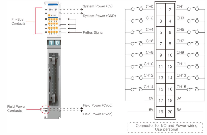
Diagram description (text version): ST-112F (16 inputs, source/negative logic, 5 V): front view with FnBus contacts (system power 5 V/GND and FnBus signal), STATUS LED, 16 channel LEDs and a 20-pin connector for I/O and power wiring. Connector pinout: pins 1–16 – inputs CH0–CH15 (odd pins CH0, CH2 … CH14, even pins CH1, CH3 … CH15), pins 17/18 – 0 V, pins 19/20 – 5 V. Each input is wired through a switch to the common line, which is connected to 0 V (pins 17/18). Field power contacts: 0 Vdc and 5 Vdc.
ST-112F – pin description
| Pin No. | Description |
|---|---|
| 1 | Input Channel 0 |
| 2 | Input Channel 1 |
| 3 | Input Channel 2 |
| 4 | Input Channel 3 |
| 5 | Input Channel 4 |
| 6 | Input Channel 5 |
| 7 | Input Channel 6 |
| 8 | Input Channel 7 |
| 9 | Input Channel 8 |
| 10 | Input Channel 9 |
| 11 | Input Channel 10 |
| 12 | Input Channel 11 |
| 13 | Input Channel 12 |
| 14 | Input Channel 13 |
| 15 | Input Channel 14 |
| 16 | Input Channel 15 |
| 17 | Field Ground (0V) |
| 18 | Field Ground (0V) |
| 19 | Field Power (+5Vdc) |
| 20 | Field Power (+5Vdc) |
3.1.5 ST-1214
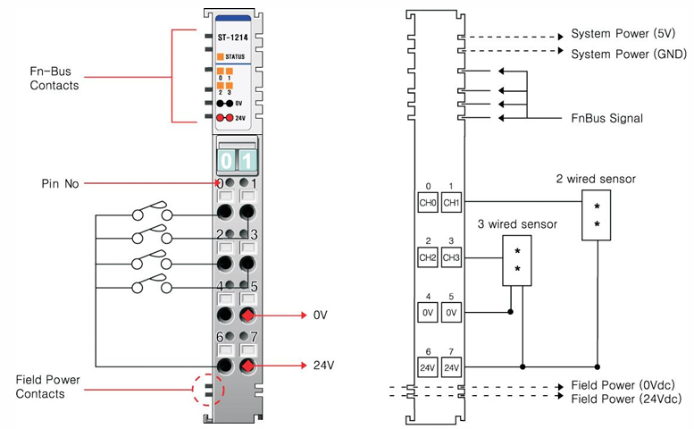
Diagram description (text version): ST-1214 (4 inputs, sink/positive logic, 24 V): front view with FnBus contacts on the left side, STATUS LED, channel LEDs 0–3 and the 8-pin terminal block. Input switches are connected between the inputs (pins 0–3) and +24 V (pins 6/7); pins 4/5 are field ground 0 V. The wiring diagram shows a 2-wire sensor between CH1 and 24 V, and a 3-wire sensor connected to CH2, 0 V and 24 V. System power (5 V, GND) and the FnBus signal come from the FnBus contacts; field power is taken from the field power contacts.
ST-1214 – pin description
| Pin No. | Description |
|---|---|
| 0 | Input Channel 0 |
| 1 | Input Channel 1 |
| 2 | Input Channel 2 |
| 3 | Input Channel 3 |
| 4 | Field Ground (0V) |
| 5 | Field Ground (0V) |
| 6 | Field Power (+24Vdc) |
| 7 | Field Power (+24Vdc) |
3.1.6 ST-1218
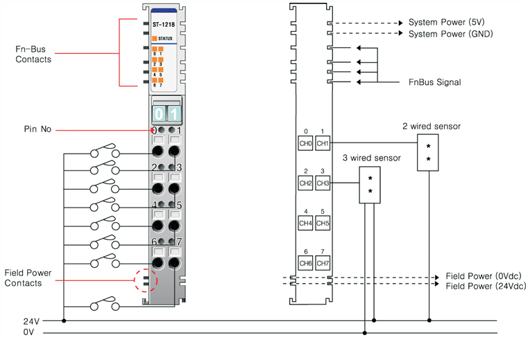
Diagram description (text version): ST-1218 (8 inputs, sink/positive logic, 24 V): front view with FnBus contacts (system power 5 V/GND and FnBus signal), STATUS LED, channel LEDs 0–7 and the 8-pin terminal block, where all pins 0–7 are inputs CH0–CH7 (no supply terminals on the module). The input switches are connected to an external 24 V line; the wiring diagram shows a 2-wire sensor between CH1 and the 24 V line, and a 3-wire sensor connected to CH2 and to the external 24 V and 0 V lines. Field power contacts: 0 Vdc and 24 Vdc.
ST-1218 – pin description
| Pin No. | Description |
|---|---|
| 0 | Input Channel 0 |
| 1 | Input Channel 1 |
| 2 | Input Channel 2 |
| 3 | Input Channel 3 |
| 4 | Input Channel 4 |
| 5 | Input Channel 5 |
| 6 | Input Channel 6 |
| 7 | Input Channel 7 |
3.1.7 ST-121F
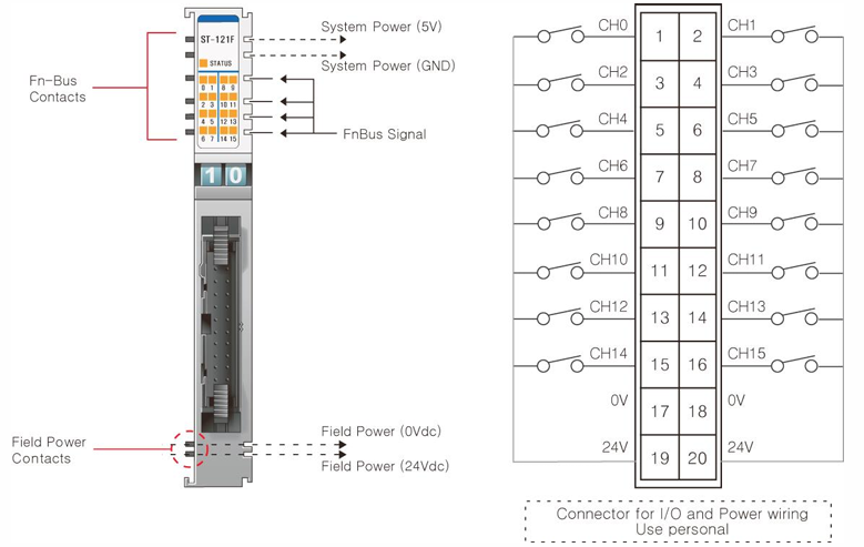
Diagram description (text version): ST-121F (16 inputs, sink/positive logic, 24 V): front view with FnBus contacts (system power 5 V/GND and FnBus signal), STATUS LED, 16 channel LEDs and a 20-pin connector for I/O and power wiring. Connector pinout: pins 1–16 – inputs CH0–CH15 (odd pins CH0, CH2 … CH14, even pins CH1, CH3 … CH15), pins 17/18 – 0 V, pins 19/20 – 24 V. Each input is wired through a switch to the common line, which is connected to 24 V (pins 19/20). Field power contacts: 0 Vdc and 24 Vdc.
ST-121F – pin description
| Pin No. | Description |
|---|---|
| 1 | Input Channel 0 |
| 2 | Input Channel 1 |
| 3 | Input Channel 2 |
| 4 | Input Channel 3 |
| 5 | Input Channel 4 |
| 6 | Input Channel 5 |
| 7 | Input Channel 6 |
| 8 | Input Channel 7 |
| 9 | Input Channel 8 |
| 10 | Input Channel 9 |
| 11 | Input Channel 10 |
| 12 | Input Channel 11 |
| 13 | Input Channel 12 |
| 14 | Input Channel 13 |
| 15 | Input Channel 14 |
| 16 | Input Channel 15 |
| 17 | Field Ground (0V) |
| 18 | Field Ground (0V) |
| 19 | Field Power (+24Vdc) |
| 20 | Field Power (+24Vdc) |
3.1.8 ST-1224
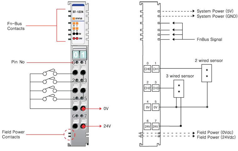
Diagram description (text version): ST-1224 (4 inputs, source/negative logic, 24 V): front view with FnBus contacts on the left side, STATUS LED, channel LEDs 0–3 and the 8-pin terminal block. Input switches are connected between the inputs (pins 0–3) and 0 V (pins 4/5); pins 6/7 are field power +24 V. The wiring diagram shows a 2-wire sensor between CH1 and 0 V, and a 3-wire sensor connected to CH2, 0 V and 24 V. System power (5 V, GND) and the FnBus signal come from the FnBus contacts; field power is taken from the field power contacts.
ST-1224 – pin description
| Pin No. | Description |
|---|---|
| 0 | Input Channel 0 |
| 1 | Input Channel 1 |
| 2 | Input Channel 2 |
| 3 | Input Channel 3 |
| 4 | Field Ground (0V) |
| 5 | Field Ground (0V) |
| 6 | Field Power (+24Vdc) |
| 7 | Field Power (+24Vdc) |
3.1.9 ST-1228
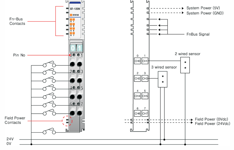
Diagram description (text version): ST-1228 (8 inputs, source/negative logic, 24 V): front view with FnBus contacts (system power 5 V/GND and FnBus signal), STATUS LED, channel LEDs 0–7 and the 8-pin terminal block, where all pins 0–7 are inputs CH0–CH7 (no supply terminals on the module). The input switches are connected to an external 0 V line; the wiring diagram shows a 2-wire sensor between CH1 and the 0 V line, and a 3-wire sensor connected to CH2 and to the external 24 V and 0 V lines. Field power contacts: 0 Vdc and 24 Vdc.
ST-1228 – pin description
| Pin No. | Description |
|---|---|
| 0 | Input Channel 0 |
| 1 | Input Channel 1 |
| 2 | Input Channel 2 |
| 3 | Input Channel 3 |
| 4 | Input Channel 4 |
| 5 | Input Channel 5 |
| 6 | Input Channel 6 |
| 7 | Input Channel 7 |
3.1.10 ST-122F
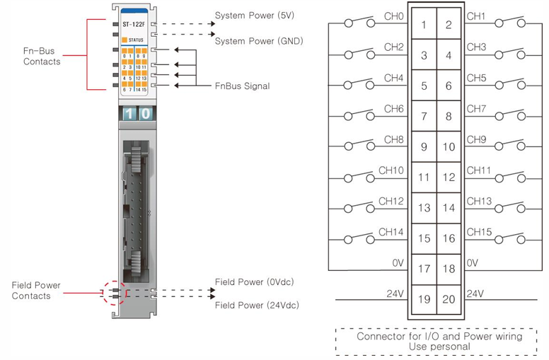
Diagram description (text version): ST-122F (16 inputs, source/negative logic, 24 V): front view with FnBus contacts (system power 5 V/GND and FnBus signal), STATUS LED, 16 channel LEDs and a 20-pin connector for I/O and power wiring. Connector pinout: pins 1–16 – inputs CH0–CH15 (odd pins CH0, CH2 … CH14, even pins CH1, CH3 … CH15), pins 17/18 – 0 V, pins 19/20 – 24 V. Each input is wired through a switch to the common line, which is connected to 0 V (pins 17/18). Field power contacts: 0 Vdc and 24 Vdc.
ST-122F – pin description
| Pin No. | Description |
|---|---|
| 1 | Input Channel 0 |
| 2 | Input Channel 1 |
| 3 | Input Channel 2 |
| 4 | Input Channel 3 |
| 5 | Input Channel 4 |
| 6 | Input Channel 5 |
| 7 | Input Channel 6 |
| 8 | Input Channel 7 |
| 9 | Input Channel 8 |
| 10 | Input Channel 9 |
| 11 | Input Channel 10 |
| 12 | Input Channel 11 |
| 13 | Input Channel 12 |
| 14 | Input Channel 13 |
| 15 | Input Channel 14 |
| 16 | Input Channel 15 |
| 17 | Field Ground (0V) |
| 18 | Field Ground (0V) |
| 19 | Field Power (+24Vdc) |
| 20 | Field Power (+24Vdc) |
3.1.11 ST-1314
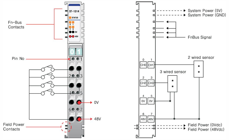
Diagram description (text version): ST-1314 (4 inputs, sink/positive logic, 48 V): front view with FnBus contacts on the left side, STATUS LED, channel LEDs 0–3 and the 8-pin terminal block. Input switches are connected between the inputs (pins 0–3) and +48 V (pins 6/7); pins 4/5 are field ground 0 V. The wiring diagram shows a 2-wire sensor between CH1 and 48 V, and a 3-wire sensor connected to CH2, 0 V and 48 V. System power (5 V, GND) and the FnBus signal come from the FnBus contacts; field power is taken from the field power contacts.
ST-1314 – pin description
| Pin No. | Description |
|---|---|
| 0 | Input Channel 0 |
| 1 | Input Channel 1 |
| 2 | Input Channel 2 |
| 3 | Input Channel 3 |
| 4 | Field Ground (0V) |
| 5 | Field Ground (0V) |
| 6 | Field Power (+48Vdc) |
| 7 | Field Power (+48Vdc) |
3.1.12 ST-131F
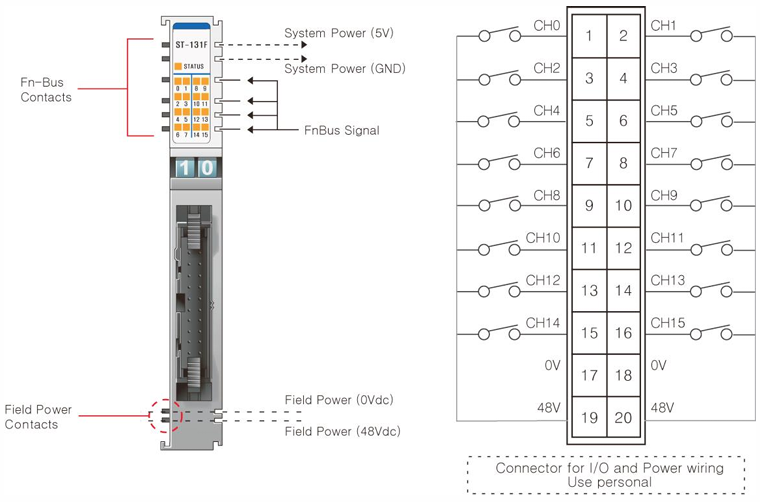
Diagram description (text version): ST-131F (16 inputs, sink/positive logic, 48 V): front view with FnBus contacts (system power 5 V/GND and FnBus signal), STATUS LED, 16 channel LEDs and a 20-pin connector for I/O and power wiring. Connector pinout: pins 1–16 – inputs CH0–CH15 (odd pins CH0, CH2 … CH14, even pins CH1, CH3 … CH15), pins 17/18 – 0 V, pins 19/20 – 48 V. Each input is wired through a switch to the common line, which is connected to 48 V (pins 19/20). Field power contacts: 0 Vdc and 48 Vdc.
ST-131F – pin description
| Pin No. | Description |
|---|---|
| 1 | Input Channel 0 |
| 2 | Input Channel 1 |
| 3 | Input Channel 2 |
| 4 | Input Channel 3 |
| 5 | Input Channel 4 |
| 6 | Input Channel 5 |
| 7 | Input Channel 6 |
| 8 | Input Channel 7 |
| 9 | Input Channel 8 |
| 10 | Input Channel 9 |
| 11 | Input Channel 10 |
| 12 | Input Channel 11 |
| 13 | Input Channel 12 |
| 14 | Input Channel 13 |
| 15 | Input Channel 14 |
| 16 | Input Channel 15 |
| 17 | Field Ground (0V) |
| 18 | Field Ground (0V) |
| 19 | Field Power (+48Vdc) |
| 20 | Field Power (+48Vdc) |
3.1.13 ST-1324
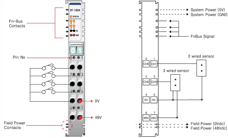
Diagram description (text version): ST-1324 (4 inputs, source/negative logic, 48 V): front view with FnBus contacts on the left side, STATUS LED, channel LEDs 0–3 and the 8-pin terminal block. Input switches are connected between the inputs (pins 0–3) and 0 V (pins 4/5); pins 6/7 are field power +48 V. The wiring diagram shows a 2-wire sensor between CH1 and 0 V, and a 3-wire sensor connected to CH2, 0 V and 48 V. System power (5 V, GND) and the FnBus signal come from the FnBus contacts; field power is taken from the field power contacts.
ST-1324 – pin description
| Pin No. | Description |
|---|---|
| 0 | Input Channel 0 |
| 1 | Input Channel 1 |
| 2 | Input Channel 2 |
| 3 | Input Channel 3 |
| 4 | Field Ground (0V) |
| 5 | Field Ground (0V) |
| 6 | Field Power (+48Vdc) |
| 7 | Field Power (+48Vdc) |
3.1.14 ST-132F
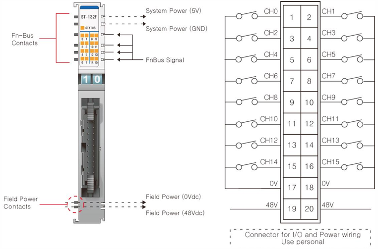
Diagram description (text version): ST-132F (16 inputs, source/negative logic, 48 V): front view with FnBus contacts (system power 5 V/GND and FnBus signal), STATUS LED, 16 channel LEDs and a 20-pin connector for I/O and power wiring. Connector pinout: pins 1–16 – inputs CH0–CH15 (odd pins CH0, CH2 … CH14, even pins CH1, CH3 … CH15), pins 17/18 – 0 V, pins 19/20 – 48 V. Each input is wired through a switch to the common line, which is connected to 0 V (pins 17/18). Field power contacts: 0 Vdc and 48 Vdc.
ST-132F – pin description
| Pin No. | Description |
|---|---|
| 1 | Input Channel 0 |
| 2 | Input Channel 1 |
| 3 | Input Channel 2 |
| 4 | Input Channel 3 |
| 5 | Input Channel 4 |
| 6 | Input Channel 5 |
| 7 | Input Channel 6 |
| 8 | Input Channel 7 |
| 9 | Input Channel 8 |
| 10 | Input Channel 9 |
| 11 | Input Channel 10 |
| 12 | Input Channel 11 |
| 13 | Input Channel 12 |
| 14 | Input Channel 13 |
| 15 | Input Channel 14 |
| 16 | Input Channel 15 |
| 17 | Field Ground (0V) |
| 18 | Field Ground (0V) |
| 19 | Field Power (+48Vdc) |
| 20 | Field Power (+48Vdc) |
3.1.15 ST-1804
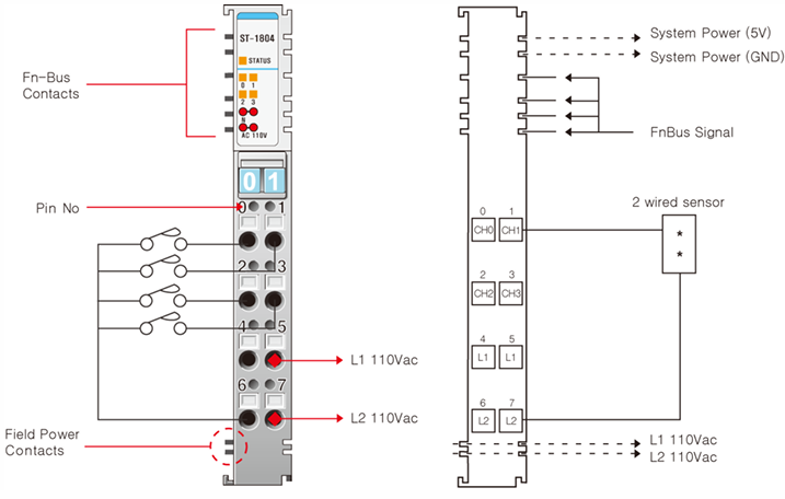
Diagram description (text version): ST-1804 (4 inputs, 110 Vac AC): front view with FnBus contacts (system power 5 V/GND and FnBus signal), STATUS LED, channel LEDs 0–3 and the 8-pin terminal block. Pins 0–3 are inputs CH0–CH3, pins 4/5 – L1 110 Vac, pins 6/7 – L2 110 Vac. The input switches are connected between the inputs and L2 (pins 6/7); the wiring diagram shows a 2-wire sensor between CH1 and L2. The field power contacts carry L1 and L2 110 Vac.
ST-1804 – pin description
| Pin No. | Description |
|---|---|
| 0 | Input Channel 0 |
| 1 | Input Channel 1 |
| 2 | Input Channel 2 |
| 3 | Input Channel 3 |
| 4 | L1 |
| 5 | L1 |
| 6 | L2 |
| 7 | L2 |
3.1.16 ST-1904
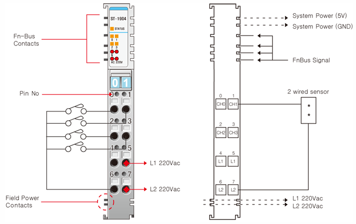
Diagram description (text version): ST-1904 (4 inputs, 220 Vac AC): front view with FnBus contacts (system power 5 V/GND and FnBus signal), STATUS LED, channel LEDs 0–3 and the 8-pin terminal block. Pins 0–3 are inputs CH0–CH3, pins 4/5 – L1 220 Vac, pins 6/7 – L2 220 Vac. The input switches are connected between the inputs and L2 (pins 6/7); the wiring diagram shows a 2-wire sensor between CH1 and L2. The field power contacts carry L1 and L2 220 Vac.
ST-1904 – pin description
| Pin No. | Description |
|---|---|
| 0 | Input Channel 0 |
| 1 | Input Channel 1 |
| 2 | Input Channel 2 |
| 3 | Input Channel 3 |
| 4 | L1 |
| 5 | L1 |
| 6 | L2 |
| 7 | L2 |
Słowa kluczowe
schemat podłączenia, przypisanie pinów, zaciski, złącze 20-pin, czujnik 2-przewodowy, czujnik 3-przewodowy, sink, source, field power, FnBus
No comments to display
No comments to display