
5. MODBUS Electrical Interface
Streszczenie: Magistrala FnBus i interfejs elektryczny MODBUS: budowa systemu FnBus i opis pinów, rezystor terminujący 120 Ω, ustawienia przełączników DIP (adres węzła – SW1, prędkość i tryb RTU/ASCII – SW2), obraz procesu I/O, mapa rejestrów i bitów MODBUS oraz przykłady obrazów wejść i wyjść w trybach skompresowanym i nieskompresowanym.
EN: FnBus system and MODBUS electrical interface: pin description, termination, DIP switch setup, process image and register/bit maps with examples.
Dotyczy: adapter sieciowy CREVIS NA-9473 (MODBUS RTU/ASCII, RS-485) systemu FnIO z modułami rozszerzeń serii ST
Źródło: dokumentacja producenta (CREVIS NA-9473 MODBUS Adapter (RS-485) User Manual); tabele przepisane z obrazów na tekst, opisy rysunków – opracowanie Multiprojekt
5.1.1 FnBus System
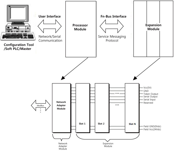
•Diagram description (text version): FnBus system structure: a configuration tool, soft PLC or master communicates over the user interface (network/serial communication – here MODBUS) with the processor module, i.e. the network adapter module. The adapter exchanges data with the expansion modules over the Fn-Bus interface (service messaging protocol). The expansion modules sit in Slot 1, Slot 2 … Slot N next to the adapter and are connected by the internal bus lines Vcc (5 V), GND, Token Output, Serial Output, Serial Input and Reserved, plus the field power lines Field GND (0 Vdc) and Field Vcc (24 Vdc).
Network Adapter Module
The Network Adapter Module forms the link between the field bus and the field devices with the Expansion Modules.
The connection to different field bus systems can be established by each of the corresponding Network Adapter Module, e.g. for SyncNet, PROFIBUS, CANopen, DeviceNet, Ethernet/IP, CC-Link, MODBUS/Serial, MODBUS/TCP etc.•
Expansion Module
The Expansion Modules are supported a variety of input and output field devices.
There are digital and analog input/output modules and special function modules.•
Two types of FnBus Message
-
- Service Messaging
- - I/O Messaging
5.2.2 FnBus Pin Description
Communication between the NA series and the expansion module as well as system / field power supply of the bus modules is carried out via the internal bus. It is comprised of 6 data pin and 2 field power pin.
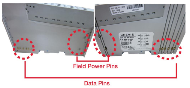
Image

version):
Photo of the sides of two FnIO modules: the row of small contacts (data pins, 6 pins) and the two separate contacts (field power pins) are marked; they connect neighbouring modules to the FnBus when the modules are pushed together.FnBus pin description
| No. | Name | Description |
|---|---|---|
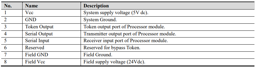
| 1 | Vcc | System supply voltage (5 V dc). |
| 2 | GND | System ground. |
| 3 | Token Output | Token output port of processor module. |
| 4 | Serial Output | Transmitter output port of processor module. |
| 5 | Serial Input | Receiver input port of processor module. |
| 6 | Reserved | Reserved for bypass token. |
| 7 | Field GND | Field ground. |
| 8 | Field Vcc | Field supply voltage (24 Vdc). |
DANGER
Do not touch data and field power pins in order to avoid soiling and damage by ESD noise.
5.3.3 MODBUS Electrical Interface
5.3.1.1 Terminator Resistor
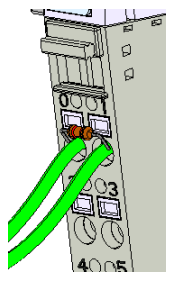
Image description (text version): Wiring of the bus termination: a 120 Ω resistor is connected between terminal 0 (RS485 DATA+) and terminal 1 (RS485 DATA−) of the NA-9473, together with the two bus wires; the second drawing shows the same as a schematic (0 DATA+ – 120 ohm – 1 DATA−).
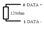
A reflection in a transmission line is the result of an impedance discontinuity that a traveling wave sees as it propagates down the line. To minimize the reflections from the end of the RS485-cable it is required to place a Line Termination near each of the 2 Ends of the Bus.
NA-9473 needs a termination resistor(120ohm) externally for more stable communication.
5.3.2.2 MODBUS DIP Switch Setup
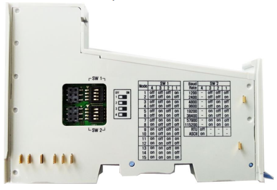
Image description (text version): Side view of the NA-9473 housing: two 4-position DIP switches – SW1 (node address) and SW2 (baud rate and RTU/ASCII protocol) – and next to them a printed label with the switch settings for node addresses 1–15 and baud rates 1200–115200 bps (the same settings are given in the tables below).
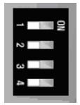
MODBUS Adapter interface configuration can be set by a DIP (4pole x 2) switch. This setup read once at power-up sequence, i.e. changes to DIP switch during operation does not affect MODBUS interface configuration.
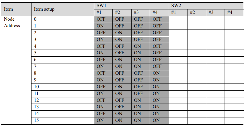
| Node
| SW1
| SW1 #2 | SW1 #3 | SW1 #4 |
|---|---|---|---|---|
| 0 | OFF | OFF | OFF | OFF |
| 1 | ON | OFF | OFF | OFF |
| 2 | OFF | ON | OFF | OFF |
| 3 | ON | ON | OFF | OFF |
| 4 | OFF | OFF | ON | OFF |
| 5 | ON | OFF | ON | OFF |
| 6 | OFF | ON | ON | OFF |
| 7 | ON | ON | ON | OFF |
| 8 | OFF | OFF | OFF | ON |
| 9 | ON | OFF | OFF | ON |
| 10 | OFF | ON | OFF | ON |
| 11 | ON | ON | OFF | ON |
| 12 | OFF | OFF | ON | ON |
| 13 | ON | OFF | ON | ON |
| 14 | OFF | ON | ON | ON |
| 15 | ON | ON | ON | ON |
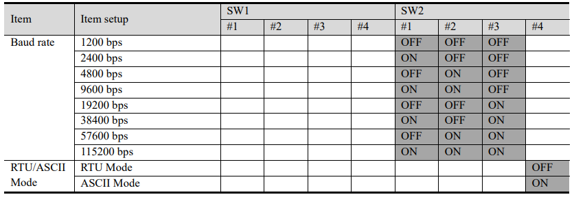

SW2 – Baud rate and RTU/ASCII mode setting (SW1 not used here)
| Item | Setting | SW2 #1 | SW2 #2 | SW2 #3 | SW2 #4 |
|---|---|---|---|---|---|
| Baud rate | 1200 bps | OFF | OFF | OFF | – |
| Baud rate | 2400 bps | ON | OFF | OFF | – |
| Baud rate | 4800 bps | OFF | ON | OFF | – |
| Baud rate | 9600 bps | ON | ON | OFF | – |
| Baud rate | 19200 bps | OFF | OFF | ON | – |
| Baud rate | 38400 bps | ON | OFF | ON | – |
| Baud rate | 57600 bps | OFF | ON | ON | – |
| Baud rate | 115200 bps | ON | ON | ON | – |
| RTU/ASCII Mode | RTU Mode | – | – | – | OFF |
| RTU/ASCII Mode | ASCII Mode | – | – | – | ON |
ATTENTION
MAC ID addresses have to be unique throughout the entire interconnected networks.
5.3.3.3 I/O Process Image Map
An expansion module may have 3 types of data as I/O data, configuration parameter and memory register. The data exchange between network adapter and expansion modules is done via an I/O process image data by FnBus protocol. The following figure shows the data flow of process image between network adapter and expansion modules.
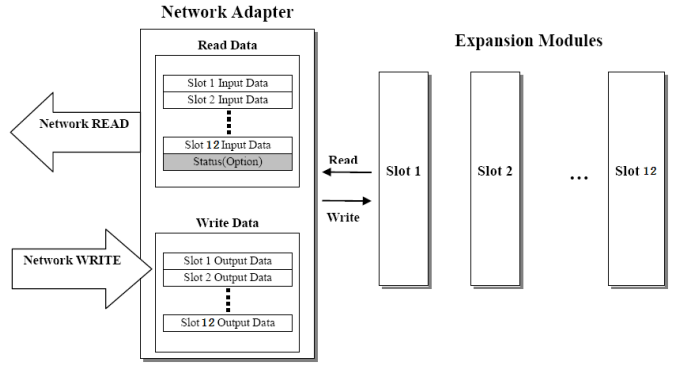
Diagram
description (text version):
Data exchange in the network adapter: the expansion modules in Slot 1 … Slot 12 are read into the “Read Data” area (Slot 1 Input Data, Slot 2 Input Data … Slot 12 Input Data, optionally followed by a status word), which the network master reads (Network READ). Data written by the master (Network WRITE) goes into the “Write Data” area (Slot 1 Output Data … Slot 12 Output Data) and is written to the expansion modules.5.3.4.4 MODBUS Interface Register / Bit Map
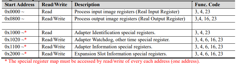
Register Map
MODBUS register map
| Start Address | Read/Write | Description | Func. Code |
|---|---|---|---|
| 0x0000 ~ | Read | Process input image registers (Real Input Register) | 3, 4, 23 |
| 0x0800 ~ | Read/Write | Process output image registers (Real Output Register) | 3, 4, 16, 23 |
| 0x1000 ~ * | Read | Adapter Identification special registers | 3, 4, 23 |
| 0x1020 ~ * | Read/Write | Adapter Watchdog, other time special registers | 3, 4, 6, 16, 23 |
| 0x1100 ~ * | Read/Write | Adapter Information special registers | 3, 4, 6, 16, 23 |
| 0x2000 ~ * | Read/Write | Expansion Slot Information special registers | 3, 4, 6, 16, 23 |
* The special register map must be accessed by read/write of every each address (one address).
Bit Map
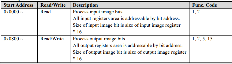
MODBUS bit map
| Start Address | Read/Write | Description | Func. Code |
|---|---|---|---|
| 0x0000 ~ | Read | Process input image bits. All input registers area is addressable by bit address. Size of input image bit is size of input image register * 16. | 1, 2 |
| 0x0800 ~ | Read/Write | Process output image bits. All output registers area is addressable by bit address. Size of output image bit is size of output image register * 16. | 1, 2, 5, 15 |
5.4 Example
5.4. Example
Input image data depends on slot position and expansion slot data type. Input process image data is only ordered by expansion slot position when input image mode is uncompressed (mode 0, 2). But, when input image mode is compressed (mode 1, 3), input process image data is ordered by expansion slot position and slot data type. Input process image mode can be set by special register 0x1114(4372). Refer to 6.3.3.
For example slot configuration
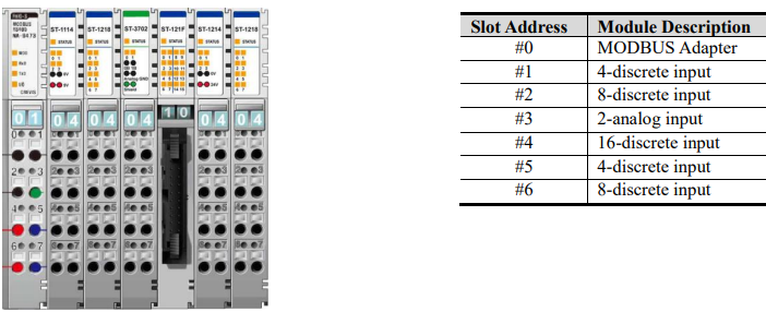
Example
slot configuration (inputs)
| Slot
| Module Description |
|---|---|
| #0 | MODBUS Adapter |
| #1 | 4-discrete input |
| #2 | 8-discrete input |
| #3 | 2-analog input |
| #4 | 16-discrete input |
| #5 | 4-discrete input |
| #6 | 8-discrete input |
- Input Process Image Mode#0 (Status(1word) + Uncompressed Input Processing Data)

| Addr. | High
| Low byte (bits #7–#0) |
|---|---|---|
| 0x0000 | bit 15 = 0, bit 14 = EC, bits 13–8 = 0 | bit 7 = 0, bits 6–0 = FnBus Status |
| 0x0001 | Discrete In 8 pts (Slot#2) | bits 7–4: empty, always 0; bits 3–0: Discrete In 4 pts (Slot#1) |
| 0x0002 | Analog Input Ch0 high byte (Slot#3) | Analog Input Ch0 low byte (Slot#3) |
| 0x0003 | Analog Input Ch1 high byte (Slot#3) | Analog Input Ch1 low byte (Slot#3) |
| 0x0004 | Discrete In high 8 pts (Slot#4) | Discrete In low 8 pts (Slot#4) |
| 0x0005 | Discrete In 8 pts (Slot#6) | bits 7–4: empty, always 0; bits 3–0: Discrete In 4 pts (Slot#5) |
- FnBus Status :
0: Normal Operation 1: FnBus Standby
2: FnBus Communication Fault 3: Slot Configuration Failed
4: No Expansion Slot
- EC (MODBUS Error Check) :
0: No Error CRC/LRC
1: Error CRC/LRC three times more sequentially since its last restart, clear counters operation, or power-up.
- Input Process Image Mode#1 (Status(1word) + Compressed Input Processing Data)
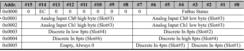
| Addr. | High
| Low byte (bits #7–#0) |
|---|---|---|
| 0x0000 | bit 15 = 0, bit 14 = EC, bits 13–8 = 0 | bit 7 = 0, bits 6–0 = FnBus Status |
| 0x0001 | Analog Input Ch0 high byte (Slot#3) | Analog Input Ch0 low byte (Slot#3) |
| 0x0002 | Analog Input Ch1 high byte (Slot#3) | Analog Input Ch1 low byte (Slot#3) |
| 0x0003 | Discrete In low 8 pts (Slot#4) | Discrete In 8 pts (Slot#2) |
| 0x0004 | Discrete In 8 pts (Slot#6) | Discrete In high 8 pts (Slot#4) |
| 0x0005 | Empty, always 0 | bits 7–4: Discrete In 4 pts (Slot#5); bits 3–0: Discrete In 4 pts (Slot#1) |
- Input Assembly Priority :
1) Analog Input Data (Word type)
2) 8 or 16 points Discrete Input Data (Byte type)
3) 4 points Input Data (Bit type)
4) 2 points Input Data (Bit type)
- Input Process Image Mode#2 (Uncompressed Input Processing Data without Status), default input image

| Addr. | High byte (bits #15–#8) | Low byte (bits #7–#0) |
|---|---|---|
| 0x0000 | Analog Input Ch0 high byte (Slot#3) | Analog Input Ch0 low byte (Slot#3) |
| 0x0001 | Analog Input Ch1 high byte (Slot#3) | Analog Input Ch1 low byte (Slot#3) |
| 0x0002 | Discrete In low 8 pts (Slot#4) | Discrete In 8 pts (Slot#2) |
| 0x0003 | Discrete In 8 pts (Slot#6) | Discrete In high 8 pts (Slot#4) |
| 0x0004 | Empty, always 0 | bits 7–4: Discrete In 4 pts (Slot#5); bits 3–0: Discrete In 4 pts (Slot#1) |
* FnBus uses the byte-oriented register mapping.
* Size of input image bit is size of input image register *16.
- Input Assembly Priority :
1) Analog Input Data (Word type)
2) 8 or 16 points Discrete Input Data (Byte type)
3) 4 points Input Data (Bit type)
4) 2 points Input Data (Bit type)
5.4.2.2 Example of Output Process Image(Output Register) Map
Output image data depends on slot position and expansion slot data type. Output process image data is only ordered by expansion slot position when output image mode is uncompressed (mode 0). But, when output image mode is compressed (mode 1), output process image data is ordered by expansion slot position and slot data type. Output process image mode can be set by special register 0x1115(4373). Refer to 6.3.3.
For example slot configuration
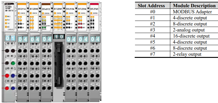
Example
slot configuration (outputs)
| Slot Address | Module Description |
|---|---|
| #0 | MODBUS Adapter |
| #1 | 4-discrete output |
| #2 | 8-discrete output |
| #3 | 2-analog output |
| #4 | 16-discrete output |
| #5 | 4-discrete output |
| #6 | 8-discrete output |
| #7 | 2-relay output |
- Output Process Image Mode#0 (Uncompressed Output Processing Data), default output image
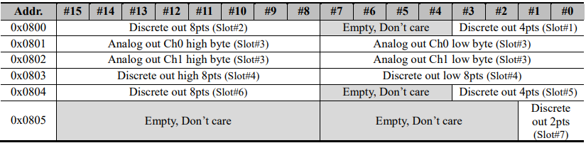
| Addr. | High byte
| Low byte (bits #7–#0) |
|---|---|---|
| 0x0800 | Discrete out 8 pts (Slot#2) | bits 7–4: empty, don’t care; bits 3–0: Discrete out 4 pts (Slot#1) |
| 0x0801 | Analog out Ch0 high byte (Slot#3) | Analog out Ch0 low byte (Slot#3) |
| 0x0802 | Analog out Ch1 high byte (Slot#3) | Analog out Ch1 low byte (Slot#3) |
| 0x0803 | Discrete out high 8 pts (Slot#4) | Discrete out low 8 pts (Slot#4) |
| 0x0804 | Discrete out 8 pts (Slot#6) | bits 7–4: empty, don’t care; bits 3–0: Discrete out 4 pts (Slot#5) |
| 0x0805 | Empty, don’t care | bits 7–2: empty, don’t care; bits 1–0: Discrete out 2 pts (Slot#7) |
- Output Process Image Mode#1 (Compressed Output Processing Data)
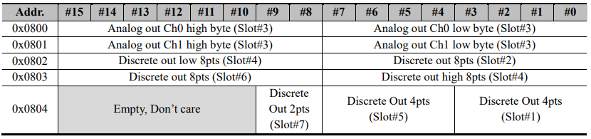
| Addr. | High byte (bits #15–#8) | Low byte (bits #7–#0) |
|---|---|---|
| 0x0800 | Analog out Ch0 high byte (Slot#3) | Analog out Ch0 low byte (Slot#3) |
| 0x0801 | Analog out Ch1 high byte (Slot#3) | Analog out Ch1 low byte (Slot#3) |
| 0x0802 | Discrete out low 8 pts (Slot#4) | Discrete out 8 pts (Slot#2) |
| 0x0803 | Discrete out 8 pts (Slot#6) | Discrete out high 8 pts (Slot#4) |
| 0x0804 | bits 15–10: empty, don’t care; bits 9–8: Discrete out 2 pts (Slot#7) | bits 7–4: Discrete out 4 pts (Slot#5); bits 3–0: Discrete out 4 pts (Slot#1) |
* FnBus uses the byte-oriented register mapping.
* Size of input image bit is size of input image register *16.
- Output Assembly Priority :
1) Analog Output Data (Word type)
2) 8 or 16 points Discrete Output Data (Byte type)
3) 4 points Output Data (Bit type)
4) 2 points Output Data (Bit type)
Słowa kluczowe
FnBus, RS-485, rezystor terminujący, 120 Ohm, DIP switch, SW1, SW2, adres węzła, baud rate, RTU, ASCII, obraz procesu, mapa rejestrów, mapa bitów, tryb skompresowany