
6. I/O Electrical Feature and Wiring
Streszczenie: Wejścia/wyjścia ID2000: optoizolowane we/wy typu V oraz nieizolowane i dwukierunkowe linie pozostałych typów – obwody wewnętrzne, parametry elektryczne, podłączenie do urządzeń PNP/NPN i przełącznika (z IO box lub rezystorem 1 kΩ) oraz port RS-232.
EN: ID2000 I/O: opto-isolated I/O of type V and non-isolated/bi-directional lines of other types – internal circuits, electrical features, wiring to PNP/NPN devices and switches (IO box or 1 kΩ resistor), and the RS-232 port.
Dotyczy: przemysłowy czytnik kodów Hikrobot serii ID2000 (typy I–VII; Fast Ethernet, USB lub RS-232; obsługa przez klienta IDMVS i kody konfiguracyjne)
Źródło: dokumentacja producenta (Hikrobot ID2000 Series Industrial Code Reader User Manual); tabele i uwagi przepisane z obrazów na tekst; opisy rysunków – opracowanie Multiprojekt
6.1 I/O Electrical Feature and Wiring of Type V Device
6.1.1 Opto-isolatedIsolated Input Circuit
Type V device's LineIn 0/1 are opto-isolated inputs, and internal circuit is as follows.
Note:
- The input voltage ranges from 5 VDC to 30 VDC.
- The breakdown voltage is 36 VDC. Keep voltage stable.
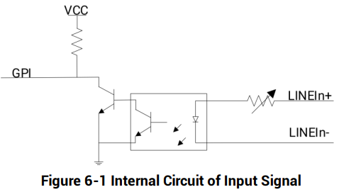
Figure 6-1 Internal Circuit of Input Signal
Figure description (text version): Schematic: the LINEIn+ and LINEIn- terminals drive the LED of an optocoupler through a current-limiting element; the optocoupler output transistor drives a transistor that pulls the GPI line (pulled up to VCC by a resistor) to ground.
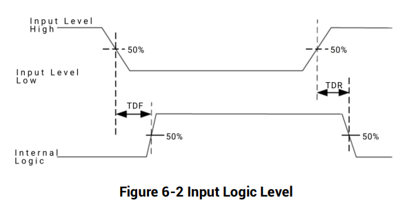
Figure 6-2 Input Logic Level
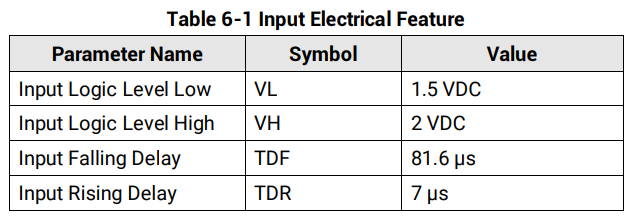
Table 6-1 Input Electrical Feature
| Parameter Name | Symbol | Value |
|---|---|---|
| Input Logic Level Low | VL | 1.5 VDC |
| Input Logic Level High | VH | 2 VDC |
| Input Falling Delay | TDF | 81.6 μs |
| Input Rising Delay | TDR | 7 μs |
6.1.2 Opto-isolatedIsolated Output Circuit
Type V device's LineOut 0/1 are opto-isolated outputs, and internal circuit is as follows.
Note:
- The output voltage ranges from 5 VDC to 30 VDC.
- The maximum output current is 25 mA.
- Do not directly connect inductive loads (e.g. DC motor) when outputting.
- If the external voltage and resistance change, the corresponding current of the output signal and output logic level low may differ.
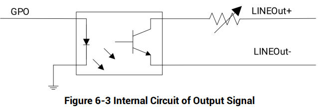
Figure 6-3 Internal Circuit of Output Signal
Figure description (text version): Schematic: the GPO signal drives the LED of an optocoupler (cathode to device ground); the optocoupler output transistor is connected between the LINEOut+ terminal (through a protection element) and LINEOut-.
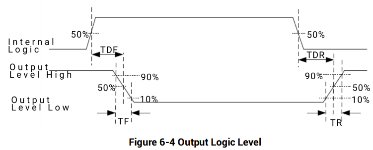
Figure 6-4 Output Logic Level
Figure
description
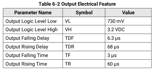
Timing diagram: upper trace – internal logic, lower trace – output level (inverted). TDF is the delay from the internal logic rising edge (50%) to the output falling edge (50%); TDR is the delay from the internal logic falling edge to the output rising edge; TF is the output fall time between 90% and 10%; TR is the rise time between 10% and 90%.
Table 6-2 Output Electrical Feature
| Parameter Name | Symbol | Value |
|---|---|---|
| Output Logic Level Low | VL | 730 mV |
| Output Logic Level High | VH | 3.2 VDC |
| Output Falling Delay | TDF | 6.3 μs |
| Output Rising Delay | TDR | 68 μs |
| Output Falling Time | TF | 3 μs |
| Output Rising Time | TR | 60 μs |
6.1.3 Input Signal Wiring
The device can receive the external input signal, and this section introduces input signal wiring.

- Input
signal
wiringmay differ by external device types.
- The voltage of VCC should be equal to or less than that of PWR. Otherwise, the output signal exception may occur.
PNP Device
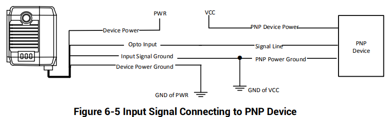
Figure 6-5 Input Signal Connecting to PNP Device
Figure description (text version): Wiring diagram: device power from PWR, device power ground to the GND of PWR. The opto input is connected to the signal line of the PNP device; the input signal ground is connected to the PNP power ground and the GND of VCC; the PNP device is powered from VCC.
NPN Device
If the VCC of NPN device is 12 VDC or 24 VDC, and the pull-up resistor of the IO box is used.
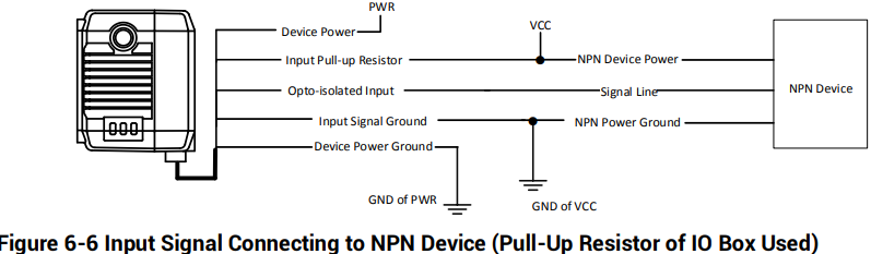
Figure 6-6 Input Signal Connecting to NPN Device (Pull-Up Resistor of IO Box Used)
Figure
descriptionIf(text version):
6.1.4 Output Signal Wiring

PNP Device
NPN DeviceIfwith the VCC of NPN device power; the opto-isolated input is 12connected VDCto orthe 24signal VDC,line of the NPN device; the input signal ground is connected to the NPN power ground and the pull-up resistorGND of the IO box is used.
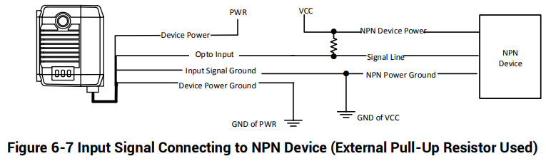
If the VCC of NPN device is 12 VDC or 24 VDC and the external pull-up resistor is used, it is recommended to use 1 KΩ pull-up resistor.
Figure 6-7 Input Signal Connecting to NPN Device (External Pull-Up Resistor Used)
Figure description (text version): Wiring diagram: device power from PWR, device power ground to the GND of PWR. The opto input is connected to the signal line of the NPN device, with an external pull-up resistor between the signal line and VCC (NPN device power); the input signal ground is connected to the NPN power ground and the GND of VCC.
6.1.4 Output Signal Wiring
Note:
- Output signal wiring may differ by external device types.
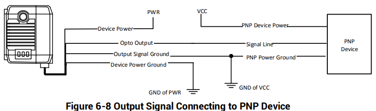
- The voltage of VCC should be equal to or less than that of PWR. Otherwise, the output signal exception may occur.
PNP Device
Figure 6-8 Output Signal Connecting to PNP Device
Figure description (text version): Wiring diagram: device power from PWR, device power ground to the GND of PWR. The opto output is connected to the signal line of the PNP device; the output signal ground is connected to the PNP power ground and the GND of VCC; the PNP device is powered from VCC.
NPN Device
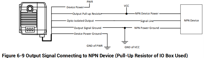
If the VCC of NPN device is 12 VDC or 24 VDC, and the pull-up resistor of the IO box is used.
Figure 6-9 Output Signal Connecting to NPN Device (Pull-Up Resistor of IO Box Used)
Figure description (text version): Wiring diagram: device power from PWR, device power ground to the GND of PWR. The output pull-up resistor line goes to VCC together with the NPN device power; the opto-isolated output is connected to the signal line of the NPN device; the output signal ground is connected to the NPN power ground and the GND of VCC.
If the VCC of NPN device is 12 VDC or 24 VDC and the external pull-up resistor is used, it is recommended to use 1 KΩ pull-up resistor.
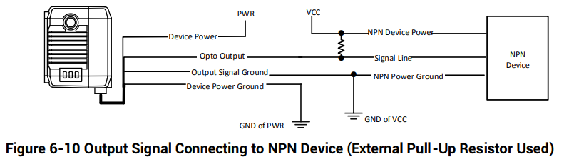
Figure 6-10 Output Signal Connecting to NPN Device (External Pull-Up Resistor Used)
Figure description (text version): Wiring diagram: device power from PWR, device power ground to the GND of PWR. The opto output is connected to the signal line of the NPN device, with an external pull-up resistor between the signal line and VCC (NPN device power); the output signal ground is connected to the NPN power ground and the GND of VCC.
6.2 I/O Electrical Feature and Wiring of Other Devices
The other devices include type I to type IV devices, and type VI and type VII devices. With different device types, their I/O electrical feature varies.●
- Type II device: Its Line 0/1/2/3 are all bi-directional signals.
● - Type I, type III, type IV and type VI devices: Their Line 2 is non-isolated input signal, Line 3 is non-isolated output signal, and Line 0/1 are both bi-directional signals.
● - Type VII device: Its LineIn 1 is non-isolated input signal, LineOut 3 is non-isolated output signal, and Line 2 is bi-directional signal.
6.2.1 Non-isolatedIsolated Input Circuit
The internal circuit of other devices’ non-isolated input signal is as follows.
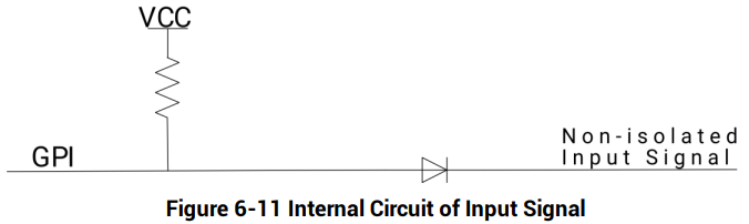
Figure 6-11 Internal Circuit of Input Signal
Figure description (text version): Schematic: the GPI line is pulled up to VCC through a resistor and connected through a diode to the non-isolated input signal terminal.
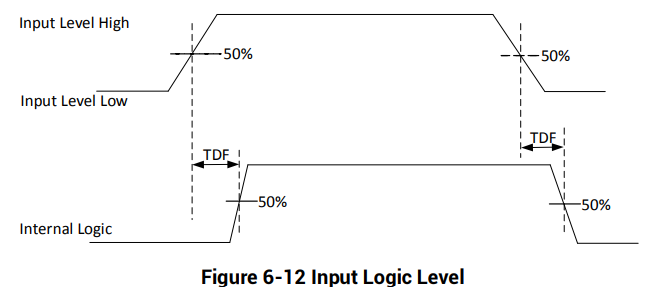
Figure 6-12 Input Logic Level
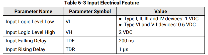
Table 6-3 Input Electrical Feature
| Parameter Name | Parameter Symbol | Value |
|---|---|---|
| Input Logic Level Low | VL | Type I, II, III and IV devices: 1 VDC Type VI and VII devices: 0.6 VDC |
| Input Logic Level High | VH | 2 VDC |
| Input Falling Delay | TDF | 200 ns |
| Input Rising Delay | TDR | 1 μs |
6.2.2 Non-isolatedIsolated Output Circuit
The internal circuit of the device’s non-isolated output signal is as follows.
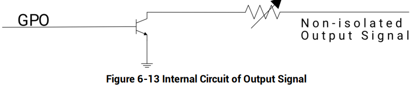
Figure 6-13 Internal Circuit of Output Signal
Figure description (text version): Schematic: the GPO signal drives the base of a transistor whose emitter is grounded; the collector is connected through a protection element to the non-isolated output signal terminal (open-collector output).
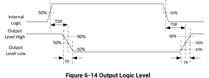
Figure 6-14 Output Logic Level
Figure description (text version): Timing diagram: upper trace – internal logic, lower trace – output level (inverted). TDF is the delay from the internal logic rising edge (50%) to the output falling edge (50%); TDR is the delay from the internal logic falling edge to the output rising edge; TF is the output fall time between 90% and 10%; TR is the rise time between 10% and 90%.
When the external voltage is 12 VDC and pull-up resistor is 1 KΩ, output electric feature is shown below.
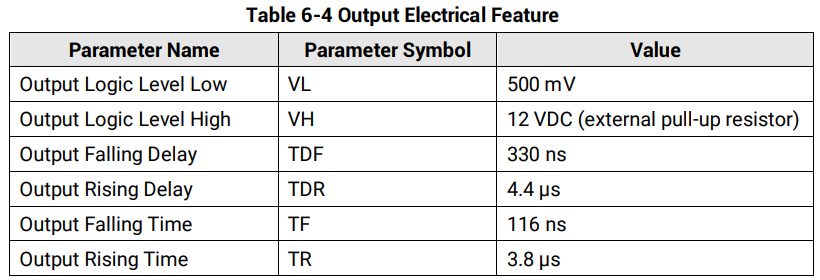
| Parameter Name | Parameter Symbol | Value |
|---|---|---|
| Output Logic Level Low | VL | 500 mV |
| Output Logic Level High | VH | 12 VDC (external pull-up resistor) |
| Output Falling Delay | TDF | 330 ns |
| Output Rising Delay | TDR | 4.4 μs |
| Output Falling Time | TF | 116 ns |
| Output Rising Time | TR | 3.8 μs |
Relation between different external voltages and output logic level low is shown below.
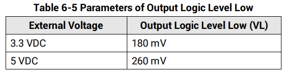
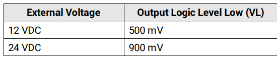
Table 6-5 Parameters of Output Logic Level Low
| External Voltage | Output Logic Level Low (VL) |
|---|---|
| 3.3 VDC | 180 mV |
| 5 VDC | 260 mV |
| 12 VDC | 500 mV |
| 24 VDC | 900 mV |
6.2.3 Bi-directionalDirectional I/O Circuit
The bi-directional signal in I/O signal can be use as input signal or output signal according to demands. Its internal circuit is shown below.
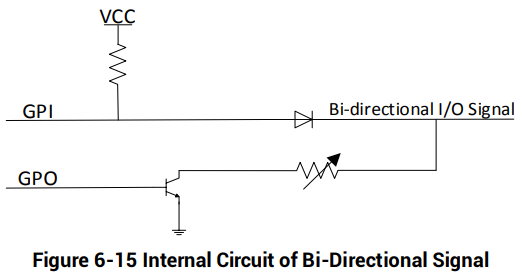
Figure 6-15 Internal Circuit of Bi-Directional Signal
Figure description (text version): Schematic: the bi-directional I/O terminal is connected to the GPI line (pulled up to VCC through a resistor) through a diode, and to the collector of the GPO output transistor (emitter grounded) through a protection element.
Configured as Input Signal
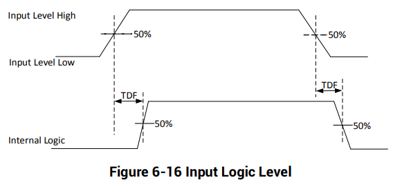
Figure 6-16 Input Logic Level
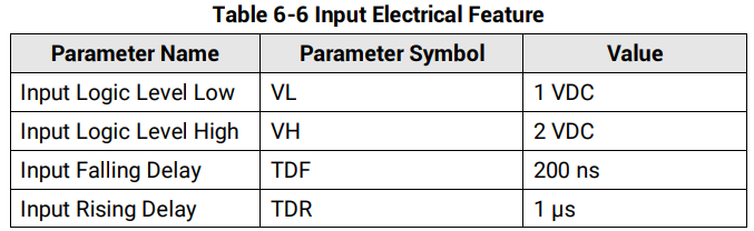
Table 6-6 Input Electrical Feature
| Parameter Name | Parameter Symbol | Value |
|---|---|---|
| Input Logic Level Low | VL | 1 VDC |
| Input Logic Level High | VH | 2 VDC |
| Input Falling Delay | TDF | 200 ns |
| Input Rising Delay | TDR | 1 μs |
Configured as Output Signal
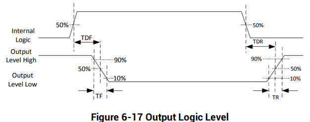
Figure 6-17 Output Logic Level
Figure description (text version): Timing diagram: upper trace – internal logic, lower trace – output level (inverted). TDF is the delay from the internal logic rising edge (50%) to the output falling edge (50%); TDR is the delay from the internal logic falling edge to the output rising edge; TF is the output fall time between 90% and 10%; TR is the rise time between 10% and 90%.
When the external voltage is 12 VDC and pull-up resistor is 1 KΩ, output electric feature is shown below.
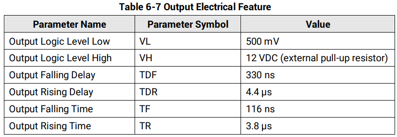
| Parameter Name | Parameter Symbol | Value |
|---|---|---|
| Output Logic Level Low | VL | 500 mV |
| Output Logic Level High | VH | 12 VDC (external pull-up resistor) |
| Output Falling Delay | TDF | 330 ns |
| Output Rising Delay | TDR | 4.4 μs |
| Output Falling Time | TF | 116 ns |
| Output Rising Time | TR | 3.8 μs |
Relation between different external voltages and output logic level low is shown below.
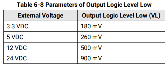
Table 6-8 Parameters of Output Logic Level Low
| External Voltage | Output Logic Level Low (VL) |
|---|---|
| 3.3 VDC | 180 mV |
| 5 VDC | 260 mV |
| 12 VDC | 500 mV |
| 24 VDC | 900 mV |
6.2.4 Input Signal Wiring
The device can receive the external input signal, and this section introduces input signal wiring.

- Input
signal
wiringmay differ by external device types.
- The voltage of VCC should be equal to or less than that of PWR. Otherwise, the output signal exception may occur.
PNP Device
Other devices apart from type VII device use the pull-down resistor of the IO box, the wiring is shown below.
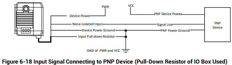
Figure 6-18 Input Signal Connecting to PNP Device (Pull-Down Resistor of IO Box Used)
Figure description (text version): Wiring diagram: device power from PWR; the PNP device is powered from VCC. The non-isolated input is connected to the signal line of the PNP device. The device power ground, the input pull-down resistor line and the PNP power ground are connected together to the common GND of PWR and VCC.
Other devices apart from type VII device use external pull-down resistor, it is recommended to use 1 KΩ pull-down resistor.
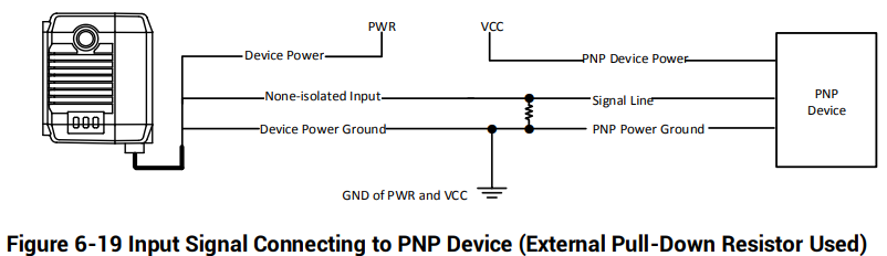
Figure 6-19 Input Signal Connecting to PNP Device (External Pull-Down Resistor Used)
Figure description (text version): Wiring diagram: device power from PWR; the PNP device is powered from VCC. The non-isolated input is connected to the signal line of the PNP device, with an external pull-down resistor between the signal line and ground. The device power ground and the PNP power ground are connected to the common GND of PWR and VCC.
Type VII device uses external pull-down resistor, it is recommended to use 1 KΩ pull-down resistor.
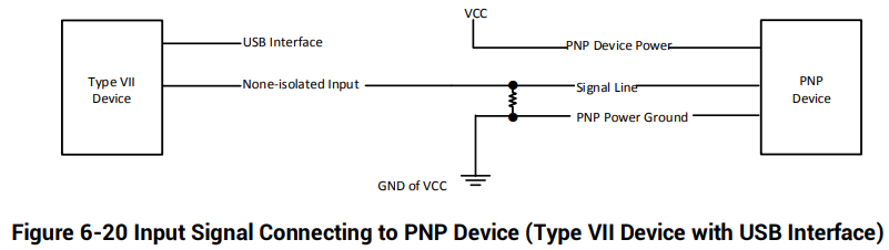
Figure 6-20 Input Signal Connecting to PNP Device (Type VII Device with USB Interface)
Figure description (text version): Wiring diagram: the type VII device is connected to the PC via its USB interface. The non-isolated input is connected to the signal line of the PNP device (powered from VCC), with an external pull-down resistor between the signal line and the PNP power ground, which is connected to the GND of VCC.
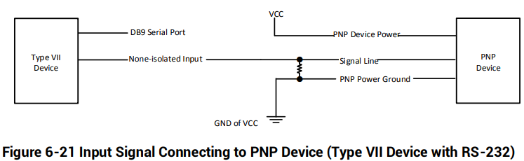
Figure 6-21 Input Signal Connecting to PNP Device (Type VII Device with RS-232)
Figure description (text version): Wiring diagram: the type VII device is connected via its DB9 serial port. The non-isolated input is connected to the signal line of the PNP device (powered from VCC), with an external pull-down resistor between the signal line and the PNP power ground, which is connected to the GND of VCC.
NPN Device
Other devices apart from type VII device use the pull-up resistor of the IO box, the wiring is shown below.
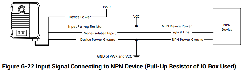
Figure 6-22 Input Signal Connecting to NPN Device (Pull-Up Resistor of IO Box Used)
OtherFigure devicesdescription apart(text version): Wiring diagram: device power from typePWR. VII device use external pull-up resistor, it is recommended to use 1 KΩ pull-up resistor.
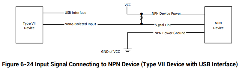
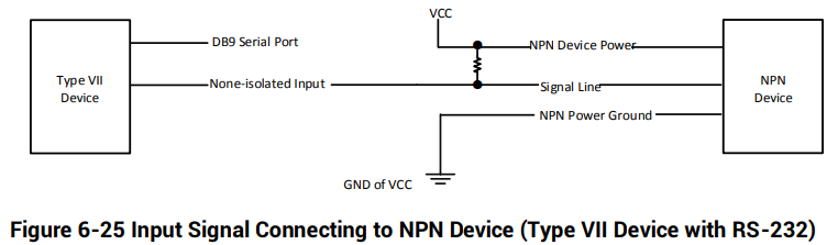
Type VII device uses external pull-up resistor, it is recommended to use 1 KΩ pull-up resistor.
Switch
The switch can provide low electrical level to trigger the bi-directional I/O.
6.2.5 Output Signal Wiring

PNP Device
NPN DeviceOther devices apart from type VII device use theinput pull-up resistor line is connected to VCC together with the NPN device power; the non-isolated input is connected to the signal line of the IONPN box,device; the wiringdevice ispower shownground below.
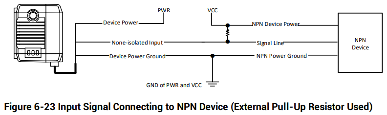
Other devices apart from type VII device use external pull-up resistor, it is recommended to use 1 KΩ pull-up resistor.
Figure 6-23 Input Signal Connecting to NPN Device (External Pull-Up Resistor Used)
Figure description (text version): Wiring diagram: device power from PWR. The non-isolated input is connected to the signal line of the NPN device, with an external pull-up resistor between the signal line and VCC (NPN device power); the device power ground and the NPN power ground go to the common GND of PWR and VCC.
Type VII device uses external pull-up resistor, it is recommended to use 1 KΩ pull-up resistor.
Figure 6-24 Input Signal Connecting to NPN Device (Type VII Device with USB Interface)
Figure description (text version): Wiring diagram: the type VII device is connected via its USB interface. The non-isolated input is connected to the signal line of the NPN device, with an external pull-up resistor between the signal line and VCC (NPN device power); the NPN power ground goes to the GND of VCC.
Figure 6-25 Input Signal Connecting to NPN Device (Type VII Device with RS-232)
Figure description (text version): Wiring diagram: the type VII device is connected via its DB9 serial port. The non-isolated input is connected to the signal line of the NPN device, with an external pull-up resistor between the signal line and VCC (NPN device power); the NPN power ground goes to the GND of VCC.
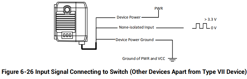
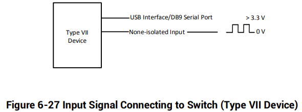
Switch
The switch can provide low electrical level to trigger the bi-directional I/O.
Figure 6-26 Input Signal Connecting to Switch (Other Devices Apart from Type VII Device)
Figure description (text version): Wiring diagram: device power from PWR; the non-isolated input receives a switched signal (pulse between 0 V and more than 3.3 V); the device power ground is connected to the common ground of PWR and VCC.
Figure 6-27 Input Signal Connecting to Switch (Type VII Device)
Figure description (text version): Wiring diagram: the type VII device is connected via its USB interface or DB9 serial port; the non-isolated input receives a switched signal (pulse between 0 V and more than 3.3 V).
6.2.5 Output Signal Wiring
Note:
- Output signal wiring may differ by external device types.
- The voltage of VCC should be equal to or less than that of PWR. Otherwise, the output signal exception may occur.
PNP Device
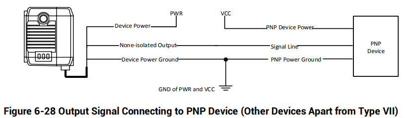
Figure 6-28 Output Signal Connecting to PNP Device (Other Devices Apart from Type VII)
Figure description (text version): Wiring diagram: device power from PWR; the PNP device is powered from VCC. The non-isolated output is connected to the signal line of the PNP device; the device power ground and the PNP power ground go to the common GND of PWR and VCC.
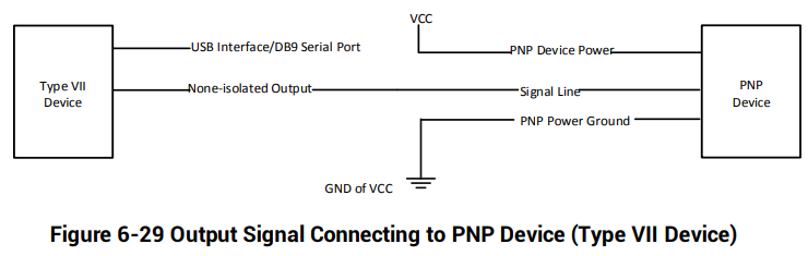
Figure 6-29 Output Signal Connecting to PNP Device (Type VII Device)
Figure description (text version): Wiring diagram: the type VII device is connected via its USB interface or DB9 serial port. The non-isolated output is connected to the signal line of the PNP device (powered from VCC); the PNP power ground goes to the GND of VCC.
NPN Device
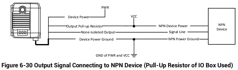
Other devices apart from type VII device use the pull-up resistor of the IO box, the wiring is shown below.
Figure 6-30 Output Signal Connecting to NPN Device (Pull-Up Resistor of IO Box Used)
Figure description (text version): Wiring diagram: device power from PWR. The output pull-up resistor line is connected to VCC together with the NPN device power; the non-isolated output is connected to the signal line of the NPN device; the device power ground and the NPN power ground go to the common GND of PWR and VCC.
Other devices apart from type VII device use external pull-up resistor, it is recommended to use 1 KΩ pull-up resistor.
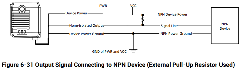
Figure 6-31 Output Signal Connecting to NPN Device (External Pull-Up Resistor Used)
Figure description (text version): Wiring diagram: device power from PWR. The non-isolated output is connected to the signal line of the NPN device, with an external pull-up resistor between the signal line and VCC (NPN device power); the device power ground and the NPN power ground go to the common GND of PWR and VCC.
Type VII device uses external pull-up resistor, it is recommended to use 1 KΩ pull-up resistor.
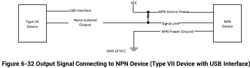
Figure 6-32 Output Signal Connecting to NPN Device (Type VII Device with USB Interface)
Figure description (text version): Wiring diagram: the type VII device is connected via its USB interface. The non-isolated output is connected to the signal line of the NPN device, with an external pull-up resistor between the signal line and VCC (NPN device power); the NPN power ground goes to the GND of VCC.
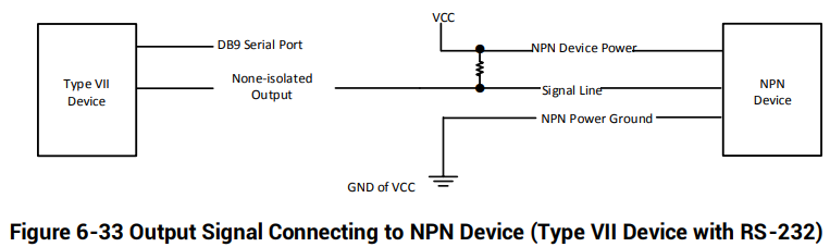
Figure 6-33 Output Signal Connecting to NPN Device (Type VII Device with RS-232)
Figure description (text version): Wiring diagram: the type VII device is connected via its DB9 serial port. The non-isolated output is connected to the signal line of the NPN device, with an external pull-up resistor between the signal line and VCC (NPN device power); the NPN power ground goes to the GND of VCC.
6.3 RS-232 Serial Port
The device supports outputting data via RS-232 serial port, and the supplied cable has a 9- pin female serial port connector. Refer to the figure and table below for pin definitions.
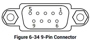
Figure 6-34 9-Pin Connector
Figure description (text version): Front view of the 9-pin D-sub serial connector: pins 1–5 in the upper row (pin 5 on the left, pin 1 on the right), pins 6–9 in the lower row (pin 9 on the left, pin 6 on the right).
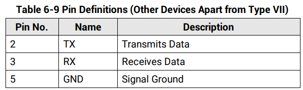
| Pin No. | Name | Description |
|---|---|---|
| 2 | TX | Transmits data |
| 3 | RX | Receives data |
| 5 | GND | Signal ground |
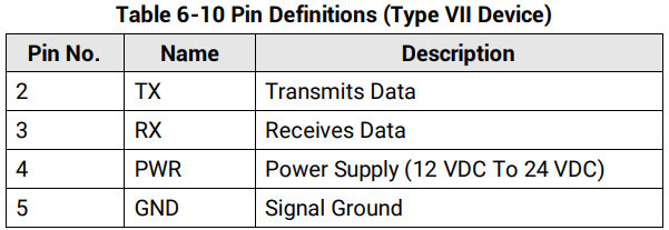
| Pin No. | Name | Description |
|---|---|---|
| 2 | TX | Transmits data |
| 3 | RX | Receives data |
| 4 | PWR | Power supply (12 VDC to 24 VDC) |
| 5 | GND | Signal ground |

Słowa kluczowe
Hikrobot ID2000, I/O wiring, opto-isolated, non-isolated, bi-directional I/O, LineIn, LineOut, PNP, NPN, pull-up, pull-down, 1 kΩ, IO box, TDF, TDR, output logic level, RS-232, DB9, wejścia, wyjścia