
3. I/O Wiring
Streszczenie: Wejścia/wyjścia czytnika ID3000: obwody i parametry elektryczne wejść LineIn i wyjść LineOut, podłączenie do urządzeń PNP/NPN i przełącznika (rezystory 330 Ω / 1 kΩ) oraz port szeregowy RS-232.
EN: ID3000 I/O: internal circuits and electrical features of LineIn inputs and LineOut outputs, wiring to PNP/NPN devices and a switch (330 Ω / 1 kΩ resistors), and the RS-232 serial port.
Dotyczy: przemysłowy czytnik kodów Hikrobot serii ID3000 (złącze M12 17-pin, Fast Ethernet, RS-232; obsługa przez klienta IDMVS)
Źródło: dokumentacja producenta (Hikrobot ID3000 Series Industrial Code Reader User Manual, V3.1.0); tabele i uwagi przepisane z obrazów na tekst, opisy rysunków – opracowanie Multiprojekt
3.1 Input Signal
The device's LineIn 0/1/2 are input signals, and their internal circuit is as follows.
Note:
- The maximum input current of input signal is 25 mA.
- The breakdown voltage is 36 VDC. Keep voltage stable.
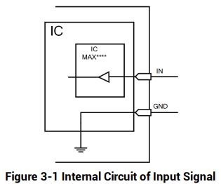
Figure 3-1 Internal Circuit of Input Signal
Figure description (text version): Schematic: the IN terminal is connected to an input buffer of the internal IC (MAX****); the GND terminal is connected to the device ground.
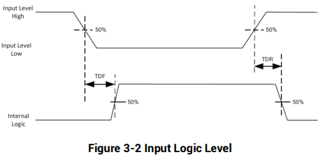
Figure 3-2 Input Logic Level
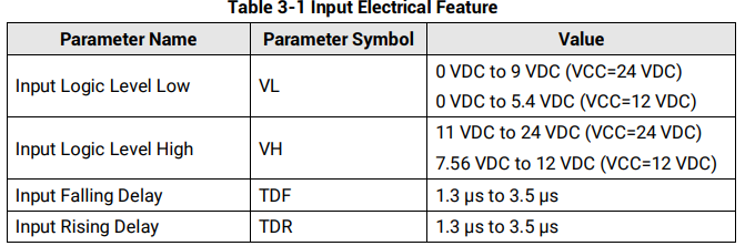

Table 3-1 Input Electrical Feature
| Parameter Name | Parameter Symbol | Value |
|---|---|---|
| Input Logic Level Low | VL | 0 VDC to 9 VDC (VCC = 24 VDC) 0 VDC to 5.4 VDC (VCC = 12 VDC) |
| Input Logic Level High | VH | 11 VDC to 24 VDC (VCC = 24 VDC) 7.56 VDC to 12 VDC (VCC = 12 VDC) |
| Input Falling Delay | TDF | 1.3 μs to 3.5 μs |
| Input Rising Delay | TDR | 1.3 μs to 3.5 μs |
Note: VCC stands for Volt Current Condenser, and it is the device’s input voltage.
3.2 Output Signal
The device's LineOut 0/1/2 are output signals, and their internal circuit is as follows.

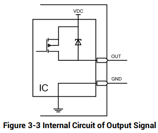
Figure 3-3 Internal Circuit of Output Signal
Figure description (text version): Schematic: a MOSFET inside the IC connects the OUT terminal to the VDC supply, with a protection diode between OUT and VDC; GND is connected to the device ground.
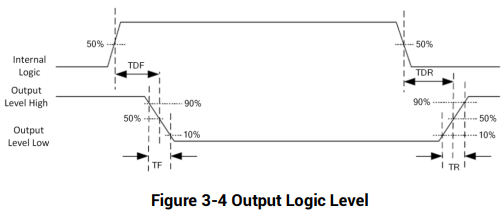
Figure 3-4 Output Logic Level
Figure description (text version): Timing diagram: upper trace – internal logic, lower trace – output level (inverted). TDF is the delay from the internal logic rising edge (50%) to the output falling edge (50%); TDR is the delay from the internal logic falling edge to the output rising edge; TF is the output fall time between 90% and 10%; TR is the rise time between 10% and 90%.
When the external voltage and resistance is 12 VDC and 1 KΩ respectively, output electrical feature is as follows.

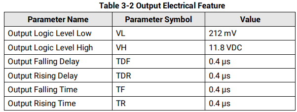
the external voltage and resistance change, the corresponding current of output signal and output logic level low may differ.
Table 3-2 Output Electrical Feature
| Parameter Name | Parameter Symbol | Value |
|---|---|---|
| Output Logic Level Low | VL | 212 mV |
| Output Logic Level High | VH | 11.8 VDC |
| Output Falling Delay | TDF | 0.4 μs |
| Output Rising Delay | TDR | 0.4 μs |
| Output Falling Time | TF | 0.4 μs |
| Output Rising Time | TR | 0.4 μs |
3.3 Input Signal Wiring
The device can receive the external input signal via I/O interface, and here we take LineIn 0 as an example to introduce input signal wiring.

PNP Device
PNPNote: DeviceIt is recommended to use 330 Ω pull-down resistor.
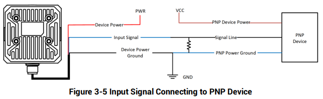
Figure 3-5 Input Signal Connecting to PNP Device
Figure description (text version): Wiring diagram: device power from PWR, device power ground to GND. The device input signal is connected to the signal line of the PNP device; a pull-down resistor is connected between the signal line and ground. The PNP device is powered from VCC and its power ground is connected to the common GND.
NPN Device
Note: If the VCC of NPN device is 12 VDC or 24 VDC, it is recommended to use 1 KΩ pull-up resistor.
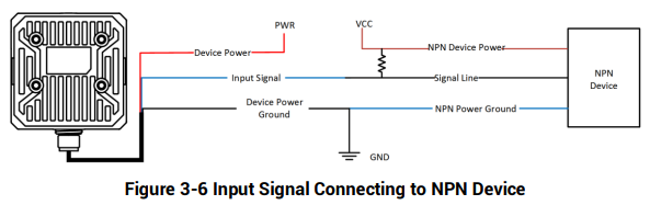
Figure 3-6 Input Signal Connecting to NPN Device
Figure description (text version): Wiring diagram: device power from PWR, device power ground to GND. The device input signal is connected to the signal line of the NPN device; a pull-up resistor is connected between the signal line and VCC (NPN device power). The NPN device power ground is connected to the common GND.
Switch
NPNNote: DeviceIt is recommended to use 330 Ω pull-down resistor.
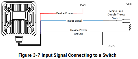
Figure 3-7 Input Signal Connecting to a Switch
Switch

3.4 Output Signal Wiring
The device can output signal to external devices via I/O interface, and here we take LineOut 0 as an example to introduce output signal wiring.

- Output
signal
wiring may differ by external device types. - The voltage of VCC should not be higher than that of PWR. Otherwise, the device’s output signal may have exception.
PNP Device
PNPNote: Device
It is recommended to use 330 Ω pull-down resistor.
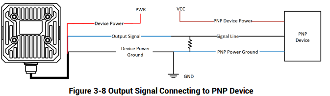
Figure 3-8 Output Signal Connecting to PNP Device
Figure description (text version): Wiring diagram: device power from PWR, device power ground to GND. The device output signal is connected to the signal line of the PNP device; a pull-down resistor is connected between the signal line and ground. The PNP device is powered from VCC; its power ground goes to the common GND.
NPN Device
Note: If the VCC of NPN device is 12 VDC or 24 VDC, it is recommended to use 1 KΩ pull-up resistor.
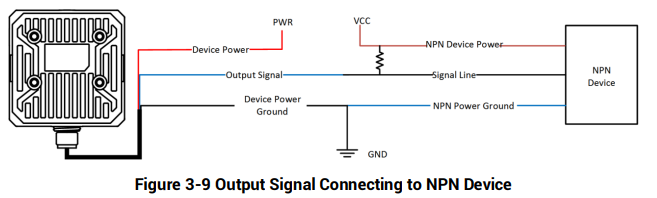
Figure
3-9
OutputSignal Connecting to NPN Device
Figure description (text version):
Wiring diagram: device power from PWR, device power ground to GND. The device output signal is connected to the signal line of the NPN device; a pull-up resistor is connected between the signal line and VCC (NPN device power). The NPN device power ground goes to the common GND.

3.5 RS-232 Serial Port
The 9-pin male connector and 25-pin male connector are commonly used serial ports, as shown below. You can refer to the table below for the specific pin name and function.
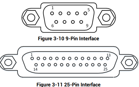
Figure 3-10 9-Pin Interface and Figure 3-11 25-Pin Interface
Figure description (text version): DB9 connector: pins 1–5 in the upper row, 6–9 in the lower row. DB25 connector: pins 1–13 in the upper row, 14–25 in the lower row.
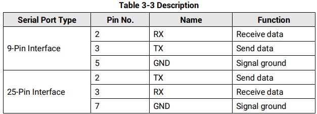
| Serial Port Type | Pin No. | Name | Function |
|---|---|---|---|
| 9-Pin Interface | 2 | RX | Receive data |
| 9-Pin Interface | 3 | TX | Send data |
| 9-Pin Interface | 5 | GND | Signal ground |
| 25-Pin Interface | 2 | TX | Send data |
| 25-Pin Interface | 3 | RX | Receive data |
| 25-Pin Interface | 7 | GND | Signal ground |
You can refer to the serial port wiring below to connect the device with an external device.
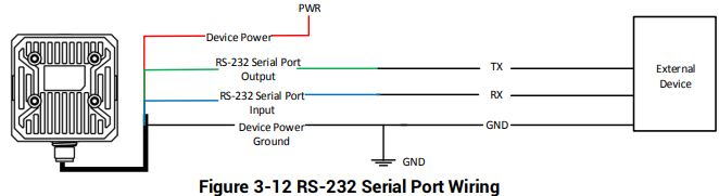
Figure 3-12 RS-232 Serial Port Wiring
Figure description (text version): Wiring diagram: device power from PWR. The RS-232 serial port output of the device goes to the TX line of the external device and the RS-232 serial port input to the RX line (as labelled in the drawing); the device power ground and the external device GND are connected to the common ground.
Słowa kluczowe
Hikrobot ID3000, I/O wiring, input signal, output signal, LineIn, LineOut, PNP, NPN, pull-up, pull-down, 330 Ω, 1 kΩ, 25 mA, 200 mA, TDF, TDR, RS-232, DB9, DB25, wejścia, wyjścia, okablowanie