
3. I/O Wiring
Streszczenie: Wejścia i wyjścia optoizolowane czytnika ID5000: obwody wewnętrzne i parametry elektryczne LineIn 0/1/2 oraz LineOut 0/1/2, podłączenie do urządzeń PNP/NPN (z rezystorem podciągającym 1 kΩ i bez) oraz port szeregowy RS-232 (DB9/DB25).
EN: ID5000 opto-isolated I/O: internal circuits and electrical features of LineIn 0/1/2 and LineOut 0/1/2, wiring to PNP/NPN devices (with and without a 1 kΩ pull-up resistor) and the RS-232 serial port (DB9/DB25).
Dotyczy: przemysłowy czytnik kodów Hikrobot serii ID5000 (złącze M12 12-pin, Gigabit Ethernet, RS-232; obsługa przez klienta IDMVS)
Źródło: dokumentacja producenta (Hikrobot ID5000 Series Industrial Code Reader User Manual, V2.5.0); tabele i uwagi przepisane z obrazów na tekst; opisy rysunków – opracowanie Multiprojekt
3.1 Input Signal
The device's LineIn 0/1/2 is opto-isolated input, and their internal circuit is as followsfollows:
Note:
- The input voltage ranges from 5 VDC to 30 VDC.
- The maximum current is 25 mA.
- The breakdown voltage is 36 VDC. Keep voltage stable.
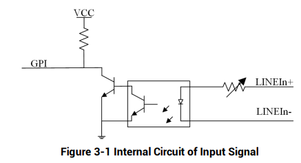
Figure 3-1 Internal Circuit of Input Signal
Figure description (text version): Schematic: the LINEIn+ and LINEIn- terminals drive the LED of an optocoupler through a current-limiting element; the optocoupler output transistor drives a transistor that pulls the GPI line (pulled up to VCC by a resistor) to ground.
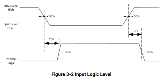
Figure 3-2 Input Logic Level
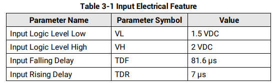
Table 3-1 Input Electrical Feature
| Parameter Name | Parameter Symbol | Value |
|---|---|---|
| Input Logic Level Low | VL | 1.5 VDC |
| Input Logic Level High | VH | 2 VDC |
| Input Falling Delay | TDF | 81.6 μs |
| Input Rising Delay | TDR | 7 μs |
3.2 Output Signal
The device's LineOut 0/1/2 is opto-isolated output, and their internal circuit is as follows.
Note:
- The output voltage ranges from 5 VDC to 30 VDC.
- The maximum current is 25 mA.
- Do not directly connect with inductive load (e.g. DC motor, etc.) when outputting.
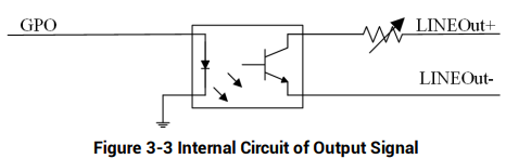
Figure 3-3 Internal Circuit of Output Signal
Figure description (text version): Schematic: the GPO signal drives the LED of an optocoupler (cathode to device ground); the optocoupler output transistor is connected between the LINEOut+ terminal (through a protection element) and LINEOut-.
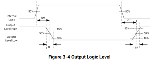
Figure 3-4 Output Logic Level

Note: If the external voltage and resistance change, the corresponding current of output signal and output logic level low may differ.
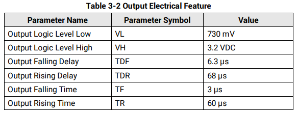
Table 3-2 Output Electrical Feature
| Parameter Name | Parameter Symbol | Value |
|---|---|---|
| Output Logic Level Low | VL | 730 mV |
| Output Logic Level High | VH | 3.2 VDC |
| Output Falling Delay | TDF | 6.3 μs |
| Output Rising Delay | TDR | 68 μs |
| Output Falling Time | TF | 3 μs |
| Output Rising Time | TR | 60 μs |
3.3 Input Signal Wiring
The device can receive external input signal via I/O interface, and here we take LineIn 0 and type I device as an example to introduce input signal wiring.

PNP Device
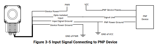
Figure 3-5 Input Signal Connecting to PNP Device
Figure description (text version): Wiring diagram: device power (Device Power+) from PWR, device power ground to the ground of PWR. The opto-isolated input is connected to the signal line of the PNP device. The input signal ground is connected to the PNP power ground and the ground of VCC; the PNP device is powered from VCC.
NPN Device
If the VCC of NPN device is 12 VDC or 24 VDC and pull-up resistor is not used, its wiring is as followsfollows:
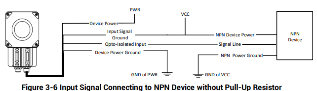
Figure 3-6 Input Signal Connecting to NPN Device without Pull-Up Resistor
Figure description (text version): Wiring diagram: device power (Device Power+) from PWR, device power ground to the ground of PWR. The input signal ground (common) is connected to VCC (NPN device power); the opto-isolated input is connected to the signal line of the NPN device; the NPN power ground is connected to the ground of VCC.
If the VCC of NPN device is 12 VDC or 24 VDC and 1 KΩ pull-up resistor is used, its wiring is as follows.
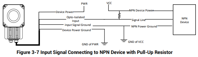
Figure 3-7 Input Signal Connecting to NPN Device with Pull-Up Resistor
Figure description (text version): Wiring diagram: device power from PWR, device power ground to the ground of PWR. The opto-isolated input is connected to the signal line of the NPN device, with a pull-up resistor between the signal line and VCC (NPN device power). The input signal ground is connected to the NPN power ground and the ground of VCC.
3.4 Output Signal Wiring
The device can output signal to external device via I/O interface, and here we take LineOut 0 and type I device as an example to introduce output signal wiring.

Note:
- Output signal wiring may differ by external device types.
- The voltage of VCC should not be higher than that of PWR. Otherwise, the device’s output signal may have exception.
PNP Device
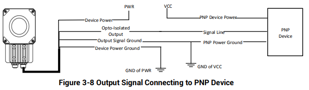
Figure 3-8 Output Signal Connecting to PNP Device
Figure description (text version): Wiring diagram: device power from PWR, device power ground to the ground of PWR. The opto-isolated output is connected to the signal line of the PNP device; the output signal ground is connected to the PNP power ground and the ground of VCC. The PNP device is powered from VCC.
NPN Device
If the VCC of NPN device is 12 VDC or 24 VDC and pull-up resistor is not used, its wiring is as follows.
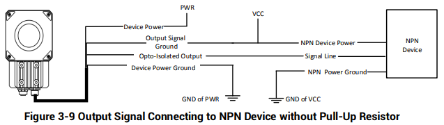
Figure 3-9 Output Signal Connecting to NPN Device without Pull-Up Resistor
Figure description (text version): Wiring diagram: device power from PWR, device power ground to the ground of PWR. The output signal ground (common) is connected to VCC (NPN device power); the opto-isolated output is connected to the signal line of the NPN device; the NPN power ground is connected to the ground of VCC.
If the VCC of NPN device is 12 VDC or 24 VDC and 1 KΩ pull-up resistor is used, its wiring
is as follows.
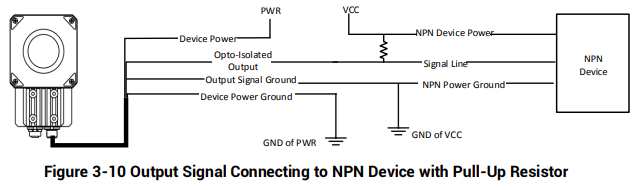
Figure 3-10 Output Signal Connecting to NPN Device with Pull-Up Resistor
Figure description (text version): Wiring diagram: device power from PWR, device power ground to the ground of PWR. The opto-isolated output is connected to the signal line of the NPN device, with a pull-up resistor between the signal line and VCC (NPN device power). The output signal ground is connected to the NPN power ground and the ground of VCC.
3.5 RS-232 Serial Port
The device supports output via RS-232 serial port. The 9-pin male connector and 25-pin male connector are commonly used serial ports, as shown below. You can refer to the table below for the specific pin name and function
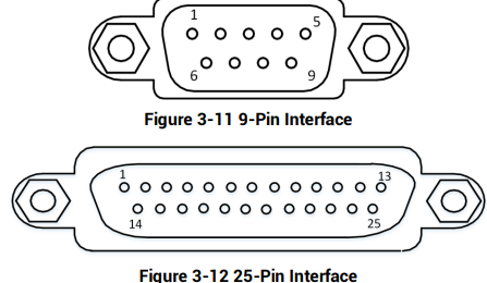
Figure 3-11 9-Pin Interface and Figure 3-12 25-Pin Interface
Figure description (text version): DB9 connector: pins 1–5 in the upper row, 6–9 in the lower row. DB25 connector: pins 1–13 in the upper row, 14–25 in the lower row.
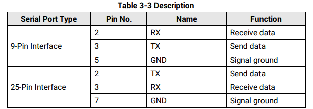
| Serial Port Type | Pin No. | Name | Function |
|---|---|---|---|
| 9-Pin Interface | 2 | RX | Receive data |
| 9-Pin Interface | 3 | TX | Send data |
| 9-Pin Interface | 5 | GND | Signal ground |
| 25-Pin Interface | 2 | TX | Send data |
| 25-Pin Interface | 3 | RX | Receive data |
| 25-Pin Interface | 7 | GND | Signal ground |
You can refer to the serial port wiring below to connect the device with an external devicedevice:
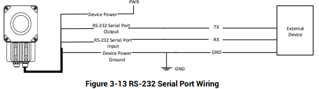
Figure 3-13 RS-232 Serial Port Wiring
Figure description (text version): Wiring diagram: device power from PWR. The RS-232 serial port output of the device goes to the TX line of the external device and the RS-232 serial port input to the RX line (as labelled in the drawing); the device power ground and the external device GND are connected to the common ground.
Słowa kluczowe
Hikrobot ID5000, I/O wiring, opto-isolated input, opto-isolated output, LineIn, LineOut, PNP, NPN, pull-up resistor, 1 kΩ, 25 mA, 5–30 VDC, TDF, TDR, RS-232, DB9, DB25, wejścia, wyjścia, okablowanie